- 您现在的位置:买卖IC网 > Sheet目录2008 > MAX1434ECQ+D (Maxim Integrated Products)IC ADC 10BIT 50MSPS 100-TQFP
MAX1434
Connect
≥ 1F (10F typ) capacitors to GND from
REFP and REFN and a
≥ 1F (10F typ) capacitor
between REFP and REFN as close to the device as
possible on the same side of the PC board.
External Reference Mode
The external reference mode allows for more control
over the MAX1434 reference voltage and allows multi-
ple converters to use a common reference. Connect
REFADJ to AVDD to disable the internal reference.
Apply a stable 1.18V to 1.30V source at REFIO. Bypass
REFIO to GND with a
≥ 0.1F capacitor. The REFIO
input impedance is > 1M
.
Clock Input (CLK)
The MAX1434 accepts a CMOS-compatible clock sig-
nal with a wide 20% to 80% input clock duty cycle.
Drive CLK with an external single-ended clock signal.
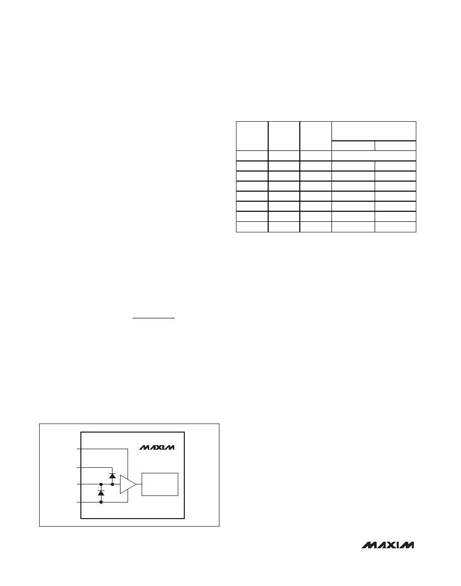
Figure 2 shows the simplified clock input diagram.
Low clock jitter is required for the specified SNR perfor-
mance of the MAX1434. Analog input sampling occurs
on the rising edge of CLK, requiring this edge to pro-
vide the lowest possible jitter. Jitter limits the maximum
SNR performance of any ADC according to the follow-
ing relationship:
where fIN represents the analog input frequency and tJ
is the total system clock jitter.
PLL Inputs (PLL1, PLL2, PLL3)
The MAX1434 features a PLL that generates an output
clock signal with 5 times the frequency of the input
clock. The output clock signal is used to clock data out
of the MAX1434 (see the
System Timing Requirements
section). Set the PLL1, PLL2, and PLL3 bits according
to the input clock range provided in Table 1.
System Timing Requirements
Figure 3 shows the relationship between the analog
inputs, input clock, frame-alignment output, serial-clock
output, and serial-data output. The differential analog
input (IN_P and IN_N) is sampled on the rising edge of
the CLK signal and the resulting data appears at the
digital outputs 6.5 clock cycles later. Figure 4 provides
a detailed, two-conversion timing diagram of the rela-
tionship between the inputs and the outputs.
Clock Output (CLKOUTP, CLKOUTN)
The MAX1434 provides a differential clock output that
consists of CLKOUTP and CLKOUTN. As shown in Figure
4, the serial output data is clocked out of the MAX1434 on
both edges of the clock output. The frequency of the out-
put clock is five times the frequency of CLK.
Frame-Alignment Output (FRAMEP, FRAMEN)
The MAX1434 provides a differential frame-alignment
signal that consists of FRAMEP and FRAMEN. As
shown in Figure 4, the rising edge of the frame-align-
ment signal corresponds to the first bit (D0) of the 10-
bit serial data stream. The frequency of the frame-
alignment signal is identical to the frequency of the
input clock.
Serial Output Data (OUT_P, OUT_N)
The MAX1434 provides its conversion results through
individual differential outputs consisting of OUT_P and
OUT_N. The results are valid 6.5 input clock cycles
after the sample is taken. As shown in Figure 3, the out-
put data is clocked out on both edges of the output
clock, LSB (D0) first. Figure 5 provides the detailed ser-
ial-output timing diagram.
SNR
ft
IN
J
=×
××
×
20
1
2
log
π
Octal, 10-Bit, 50Msps, 1.8V ADC
with Serial LVDS Outputs
14
______________________________________________________________________________________
MAX1434
DUTY-CYCLE
EQUALIZER
AVDD
CVDD
CLK
GND
Figure 2. Clock Input Circuitry
INPUT CLOCK RANGE
(MHz)
PLL1
PLL2
PLL3
MIN
MAX
0
Unused
0
1
39.0
50.0
0
1
0
27.0
39.0
0
1
19.5
27.0
1
0
13.5
19.5
1
0
1
9.8
13.5
1
0
6.8
9.8
1
4.8
6.8
Table 1. PLL1, PLL2, and PLL3
Configuration Table
发布紧急采购,3分钟左右您将得到回复。
相关PDF资料
MAX1444EHJ+T
IC ADC 10BIT 40MSPS 32-TQFP
MAX1499ECJ+
IC ADC 3 1/2DIG W/LED DVR 32TQFP
MAX152EPP+
IC ADC 8BIT 1UA PWR-DWN 20-DIP
MAX153EPP+
IC ADC 8BIT 1MSPS HI-SPD 20-DIP
MAX154AENG+
IC ADC 8BIT 4CH W/MUX&REF 24-DIP
MAX155AEPI+
IC ADC 8BIT 8CH T/H&REF 28-DIP
MAX157AEUA+
IC ADC 10BIT 108KSPS 2CH 8-UMAX
MAX160CPN+
IC ADC 8BIT UP COMPATIBLE 18-DIP
相关代理商/技术参数
MAX1434ECQ+TD
功能描述:模数转换器 - ADC 10-Bit 8Ch 50Msps 1.8V High Speed ADC RoHS:否 制造商:Texas Instruments 通道数量:2 结构:Sigma-Delta 转换速率:125 SPs to 8 KSPs 分辨率:24 bit 输入类型:Differential 信噪比:107 dB 接口类型:SPI 工作电源电压:1.7 V to 3.6 V, 2.7 V to 5.25 V 最大工作温度:+ 85 C 安装风格:SMD/SMT 封装 / 箱体:VQFN-32
MAX1434ECQ-D
功能描述:模数转换器 - ADC RoHS:否 制造商:Texas Instruments 通道数量:2 结构:Sigma-Delta 转换速率:125 SPs to 8 KSPs 分辨率:24 bit 输入类型:Differential 信噪比:107 dB 接口类型:SPI 工作电源电压:1.7 V to 3.6 V, 2.7 V to 5.25 V 最大工作温度:+ 85 C 安装风格:SMD/SMT 封装 / 箱体:VQFN-32
MAX1434ECQ-TD
功能描述:模数转换器 - ADC RoHS:否 制造商:Texas Instruments 通道数量:2 结构:Sigma-Delta 转换速率:125 SPs to 8 KSPs 分辨率:24 bit 输入类型:Differential 信噪比:107 dB 接口类型:SPI 工作电源电压:1.7 V to 3.6 V, 2.7 V to 5.25 V 最大工作温度:+ 85 C 安装风格:SMD/SMT 封装 / 箱体:VQFN-32
MAX1434EVKIT
功能描述:数据转换 IC 开发工具 Evaluation Kit for the MAX1434 MAX1436 MAX1437 MAX1438 RoHS:否 制造商:Texas Instruments 产品:Demonstration Kits 类型:ADC 工具用于评估:ADS130E08 接口类型:SPI 工作电源电压:- 6 V to + 6 V
MAX1436BECQ
制造商:Rochester Electronics LLC 功能描述: 制造商:Maxim Integrated Products 功能描述:
MAX1436BECQ+D
制造商:Maxim Integrated Products 功能描述:ADC OCTAL PIPELINED 40MSPS 12-BIT SERL - Rail/Tube
MAX1436BECQ+TD
制造商:Maxim Integrated Products 功能描述:OCTAL 12BIT 40MSPS ADC - Tape and Reel
MAX1436ECQ
制造商:Rochester Electronics LLC 功能描述: 制造商:Maxim Integrated Products 功能描述: